 NVIDIA
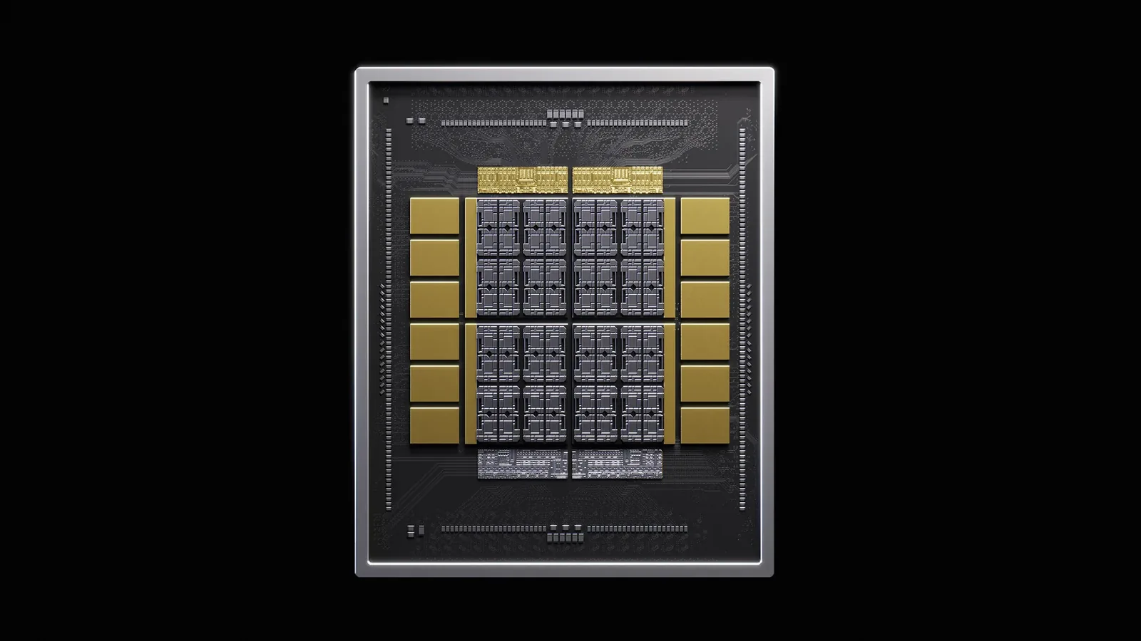
NVIDIA introduced NVLink Fusion and NVHBM on August 26, 2026, as a package-level and rack-scale approach for hyperscalers and AI-native companies building custom accelerators, or XPUs. The company positions NVLink Fusion as the connective technology and IP that lets those organizations deploy custom XPUs and CPUs into the NVIDIA AI infrastructure platform, using the scale-up and scale-out technology stack and MGX rack-scale architecture.
NVHBM is a custom HBM base-die technology that NVIDIA says it designed and validated with leading memory vendors. The company claims three main platform-level advantages over standard HBM4e: up to 30% more memory bandwidth per stack, up to 25% more compute die area, and up to 15% lower HBM power usage. These improvements target memory-bound AI workloads, where higher bandwidth can improve accelerator utilization and throughput, especially during large-model inference where moving model weights and KV-cache data between HBM and compute cores is a bottleneck.
The area savings come from a redesigned physical memory interface. Standard HBM relies on wider interface connections that increase package footprint. NVHBM moves the memory controller into the 3D HBM stack and integrates a custom PHY, reducing PHY and support area by up to 67% compared with the JEDEC HBM4e standard. The narrower interface also simplifies interposer routing, providing up to 80% more usable silicon across the layout. NVIDIA says this reclamation can free up to 30% more main-die silicon for compute or other features, giving XPU designers room to add capabilities within a fixed package footprint.
Power savings compound at scale. NVIDIA says 15% lower HBM power usage compared with standard HBM4e creates power and thermal headroom that can support up to 15,000 additional XPUs in a 1-gigawatt data center using 2,000W XPUs. At the XPU level, lower HBM power can improve performance per watt and allow more compute or higher sustained utilization. At the rack level, it reduces pressure on power delivery and cooling systems.
NVLink Fusion connects XPUs into a single scale-up domain via the NVLink Fusion chiplet, which bridges custom XPUs and the NVLink fabric. NVIDIA describes NVLink as now in its sixth generation and the only proven, purpose-built scale-up networking fabric for AI factories. Upstream, XPUs can connect to CPUs via NVLink-C2C. This scale-up domain is critical for advanced routing techniques like expert parallelism or WideEP, where different experts reside on different GPUs and require high-speed synchronization across the rack.
NVIDIA claims that combining NVLink Fusion with NVHBM delivers a 30% overall end-to-end performance increase per XPU, compounding the bandwidth, area, and power improvements at rack scale. The company also says NVLink Fusion simplifies operations across the data center, enables flexible reprovisioning of capacity, and allows custom AI XPUs to integrate with GPUs for heterogeneous compute.
For inference engineers and edge AI builders, the practical takeaway is that custom XPU designs may soon have access to a validated memory base die and a scale-up fabric that reduces integration and qualification bottlenecks. The bandwidth and area gains could help serve larger models and read KV cache faster, while the power savings could ease data center constraints. However, these are NVIDIA's claims, not independent measurements, and the actual benefits will depend on how the technology performs in real deployments.
Sources & references
NVIDIA: NVIDIA NVLink Fusion Brings NVHBM to Next-Generation AI Infrastructure ↗Source consulted: 2026-10-15